
To design JK Master-Slave Flip-Flop design using elementary gates.
Master Slave is a type of JK flip flop in which race around condition problem is removed. In this flip flop there is two stage first stage is Master and second is Slave.
Race around Condition: Toggling more than once within a clock cycle.
where,
→ tp = pulse width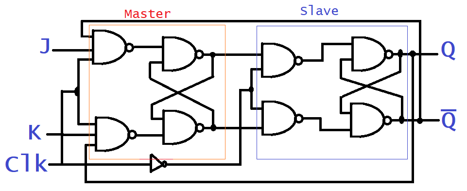
As shown in above Figure there is a clock(CLK) which is
connected to first stage(Master) and via
inverter to second stage(Slave) i.e., if clock is 1 then first stage gets 1 and second stage
gets 0.
When clock is 1 at that instant stage 1 is on and stage 2 is off and when 0,
stage
1 is off and stage 2 is on. And due to this action the output of first stage transferd to
stage
2 when first stage is off and second stage is on and hence the race around condition is
removed.
| clk | J | K | Q | Q' |
|---|---|---|---|---|
| ↑ | 0 | 0 | Previous | |
| ↑ | 0 | 1 | 0 | 1 |
| ↑ | 1 | 0 | 1 | 0 |
| ↑ | 1 | 1 | Toggle | |
To find next state
Q(n+1) = J*Q'(n) + K'*Q(n)
Where,
This animation shows the working of the JK Master-Slave Flip-Flop.
Task: Re-create the JK Master-Slave circuit by connecting the nodes. Click an output node (orange) and its valid input nodes (blue) will glow. The simulator will only activate once all 21 wires are correctly connected.
First, build the circuit in the simulator. Once complete, test all J/K combinations. The table will automatically record the output.
| Clock Pulse (CLK) | Input (J) | Input (K) | Observed Output (Q) | Observed Output (Q') | Remarks (Condition) |
|---|---|---|---|---|---|
| ↑ | 0 | 0 | |||
| ↑ | 0 | 1 | |||
| ↑ | 1 | 0 | |||
| ↑ | 1 | 1 |
Please complete the "Observations" table by building the circuit and running the simulator for all four J/K combinations. The result will appear here.
To ensure you get the correct results from the simulator, please follow these precautions. Click on each item to expand.
You must click an **orange** (output) node first. The correct **blue** (input) nodes will begin to glow, guiding your connection.
After the circuit is built, always set your desired J and K input values *before* you click the Pulse CLK button.
If you get stuck or make a mistake, use the "Reset Wires" button. This will clear all wires and restart the simulation, allowing you to try again.
To confirm the experiment, you must test all four possible input combinations *after* the circuit is complete.